Diamond-based applications
Nanoindentation using combined STM technique with Berkovich conductive diamond tip
The possibilities to use diamond nanotools for making elements of nanoelectronics have been proposed.
Nanoscale experiments & nanofabrications
with conductive diamond tip (CDT) that include processing, visualization and tunneling spectroscopy of the surface. Fabrication and characterization of nanostructures for nanoelectronics, data storages and biology are proposed
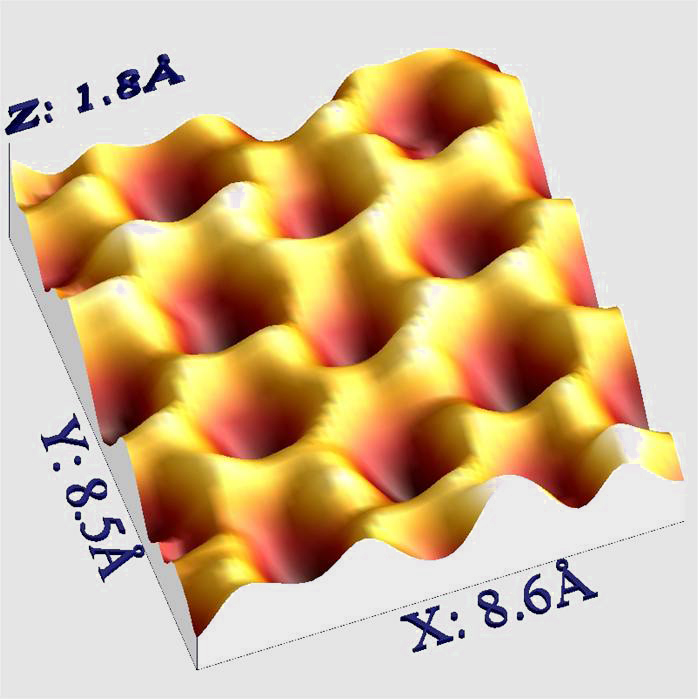
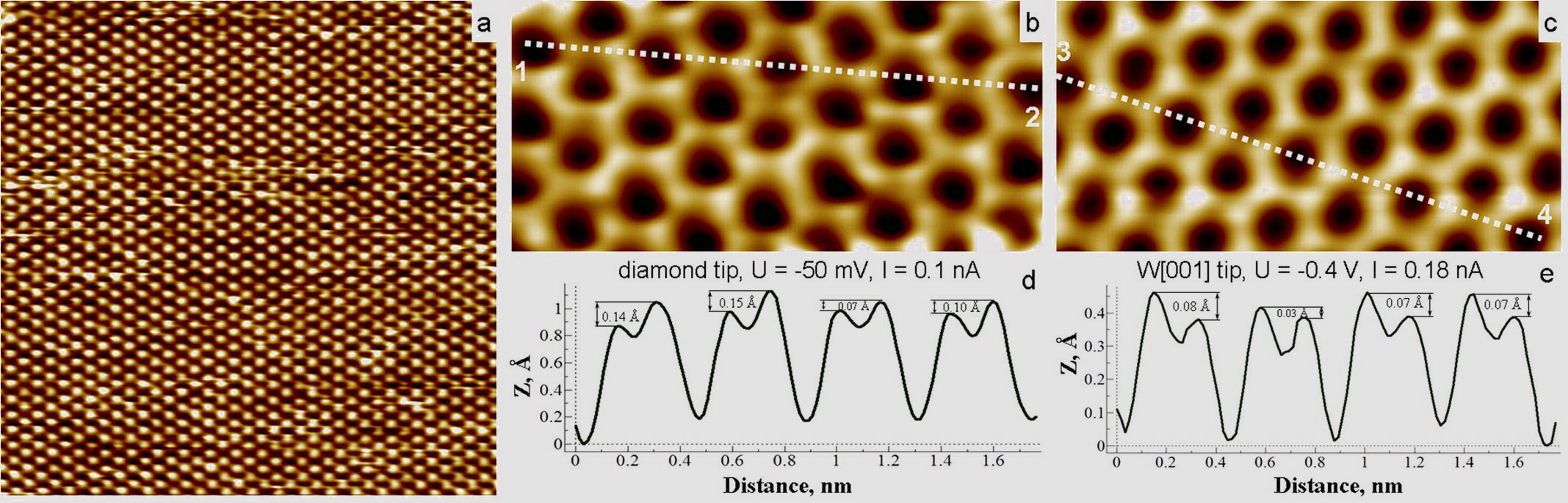
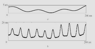
Atomically resolved STM imaging
Extremely high resolution surface imaging can be achieved in scanning tunneling microscopy (STM) experiments with diamond probes at very small tunneling gaps comparable with inter-atomic distances in solids. Conductive diamond tips can provide both spatially localized electron orbitals at the apex atom and enhanced tip stability at small tip-sample separations.
 Nanotechnology 2014.
The results of STM experiments, density functional theory calculations of the tip and surface electronic structure, and first principles tunneling current calculations demonstrate that the highest spatial resolution can be achieved with diamond tips at tip-sample distances of 3-5 angstroms when the pz orbital of the tip provides its maximum contribution to the tunneling current.
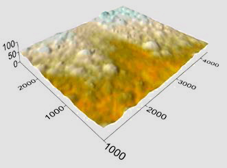
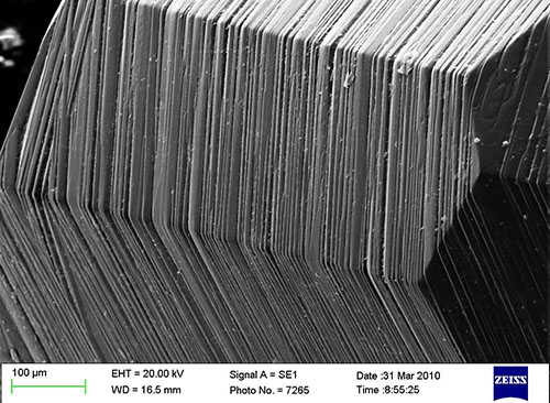
Express method of testing diamond plates
Classification of type IIa diamonds under three subclasses according to the nitrogen concentration for Electronic Nose Technique In Explosives Detection and ionising radiation detectors.
High-density data storage
A novel technique for high-density data storage that combines heat-assisted magnetic recording (HAMR) with diamond-based scanning tunneling microscopy (STM) has been proposed.
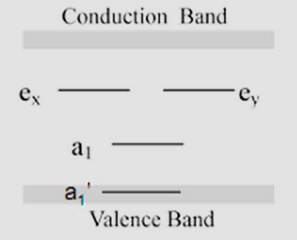
Diamond based quantum electronics
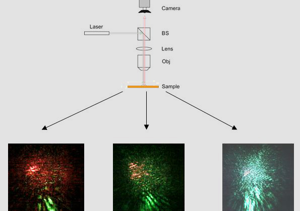
Nitrogen-vacancy (NV) centers in diamond have been extensively studied as a single-photon detection system for quantum optics applications.
Hardware
It's Interesting
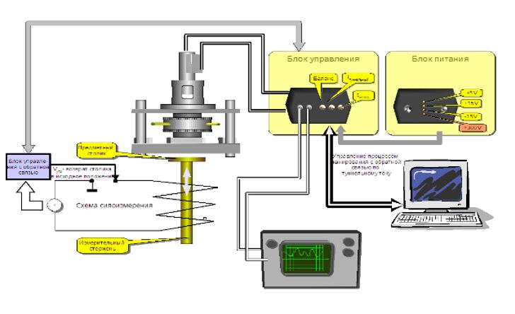
Specific features of the device are a tip of boron-doped diamond single crystal and electromagnetic system of measuring a nanointeraction between the tip and sample surface.
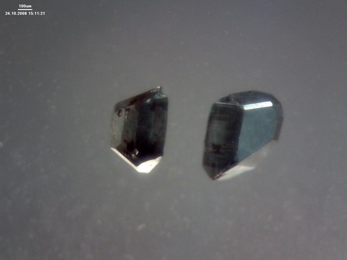
Boron-dopped diamonds.
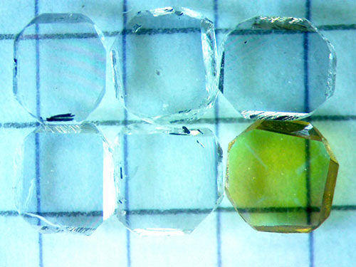
Colorness and near colorness diamond plates.
Diamond hybrid conductor/isolator.
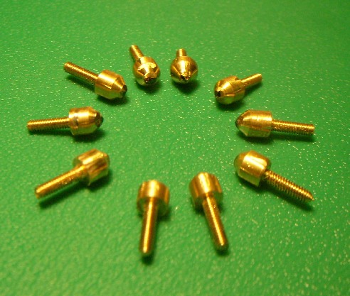
Set of SPM probes equipped with diamond tips.Apart from Homebuilt SPM nanotechnology devices our department has Nanoindenter-II? and Camscan?
Software
It's Interesting
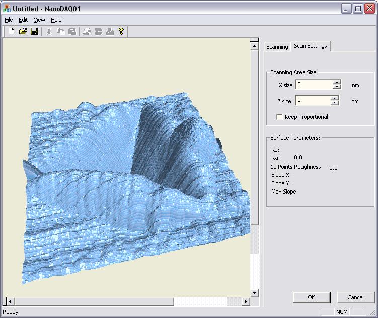
The software is specially developed to the requirements of nano-machining and data analysis.