Simulation of diamond systems
| Diamond Type | Application | Approach | Calculation method | Literature |
|---|---|---|---|---|
| IIb (B<1000 ppm) (N<0.1 ppm) |
SPM | Perturbation theory,
nonperturbative approach, LCAO |
Matching procedure, DFT method Package VASP | V Grushko, O Lűbben, A N Chaika, N Novikov, O Lysenko et al. Nanotechnology 25 (2014) |
| IIa (B<0.1 ppm) (N<0.1 ppm) Ia+IIb |
NV-centers quantum optics, quantum computer nanoelectronics | Approximation of strong coupling, group theory, LCAO | DFT method Package Abinitio | M Doherty et al. New Journal of Physics 13 (2011) |
| IIa (B<0.1 ppm) (N<0.1 ppm) |
Particle detectors | The relativistic approach Shockley-Ramo theorem, Electrodynamics | Monte Carlo method Package FLUKA | Moritz Guthoff et al. Nuclear instruments and Methods in Physics Research A735 (2014) |
Most Interesting
Tunneling current calculations
The diamond tip is modeled as a set of non-interacting, semi-infinite chains (c). The tunneling current is calculated on the basis of the Lippmann-Schwinger (LS) formalism [6]. The surface is simulated by Green's function, which is included in the LS-equation. The presence of boron atoms at the apex is not considered because the boron concentration does not exceed 0.1% and the probability of its appearance at the apex does not exceed 0.01
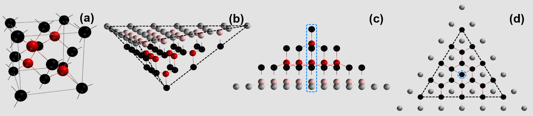
(a) The diamond unit cell. Red spheres represent the atoms lying along the diagonals of the cubic structure. (b) The atomic structure of the apex of a diamond probe. The red and black spheres show the positions of the 29 atoms used in calculating the tunneling current, while the grey spheres are present only to emphasise the pyramidal shape. (c) Side view of the diamond tip's apex. Highlighted by a blue dotted line is a single semi-infinite chain. (d) Top view of the tip apex model.
$$I_{t} ={4e^{2} V\over \hbar } \sum _{i}Im\lambda _{i}{\mathop{D}\limits^{\wedge }[\mathop{D']}\limits^{\wedge } \rho _{L} (\vec{r}_{0_{i}} ,\vec{r}_{0_{i}} )\over \left|1+\lambda _{i} \mathop{D}\limits^{\wedge } [\mathop{D']}\limits^{\wedge } *\delta g_{L} (\vec{r}_{0_{i}} ,\vec{r}_{0_{i}}^{} )\right|^{2} } $$
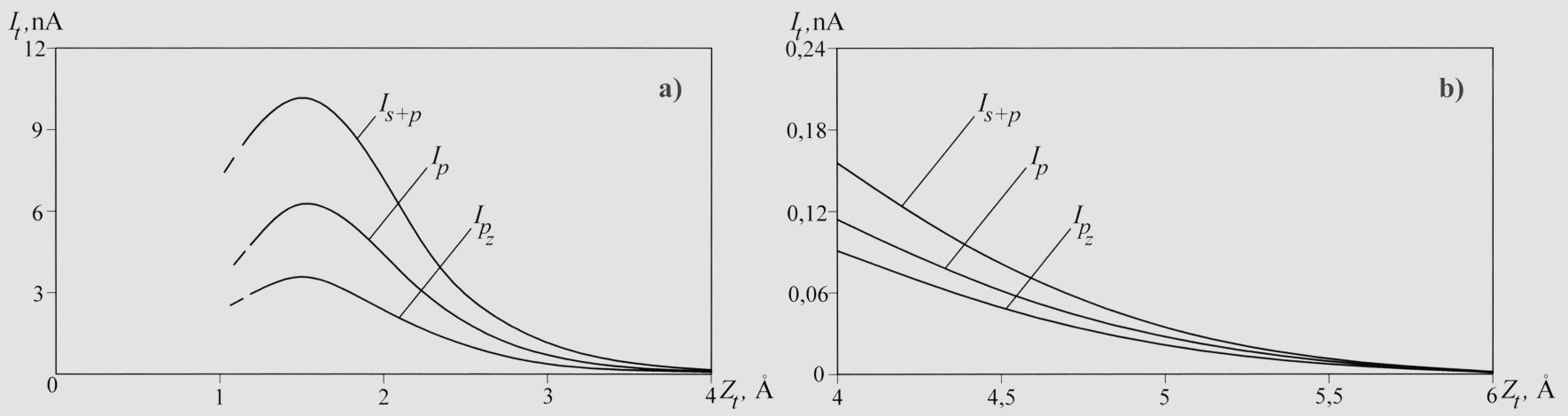
The dependence of the tunneling current It on the distance Zt between the diamond probe and the graphite surface at a sample bias voltage of 0.1 V. Is+p – total tunneling current It, taking into account both s and p electrons. Ip and Ipz are partial currents due to only the p and pz electrons, respectively. At small distances (a) the tunneling current reaches a maximum, due to the reflection of electrons from the tip at small gaps. At distances above 4 Å (b) the majority of the current is going through the pz orbital of the tip atom.Local density of states (LDOS):
$$\rho _{L} =\sum \left|\Psi _{L} \right|^{2} \delta (E-E_{\nu } )$$
Operator:$$\mathop{D}\limits^{\wedge } ={(2l+1)!!\over l!} (ik)^{-l} \int d\Omega Y_{l,m} ^{*} (\mathop{\vec{u}}\limits^{\wedge } ){\partial ^{l} \over r^{l} } $$
Green's function:$$\delta g_{L} (\vec{r},\vec{r}_{0} )={m\over 2\pi \hbar ^{2} } r(0){\exp (-k\sqrt{\rho ^{2} +(z+z_{0_{i} } )^{2} } )\over \sqrt{\rho ^{2} +(z+z_{0_{i} } )^{2} } } $$
DFT calculations of the diamond tip-graphite surface system
 The PDOS of the tip and surface atoms is modified at tip-sample distances below 3.0 Å by the overlap of the tip and surface pz-orbitals. At larger distances the pz-orbitals of the carbon atoms are responsible for STM imaging. The β atoms’ DOS at the Fermi level is larger by ~25%, and this difference decreases if the DOS is integrated over a wider range of electron energies. This difference is responsible for the two non-equivalent sublattices of carbon atoms in the atomically resolved STM images with a honeycomb pattern.
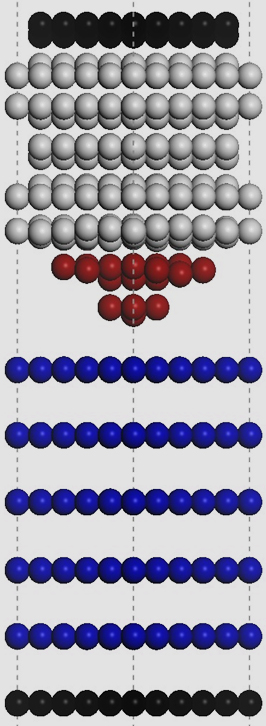
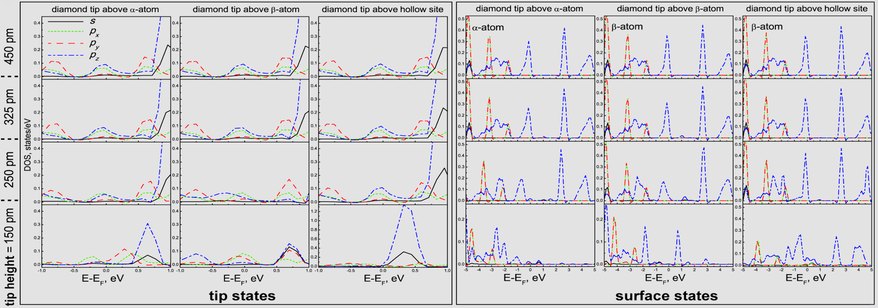 PDOS of the diamond tip (left panel) and the α and β atoms of the graphite (0001) surface (right panel) at different tip-sample distances and lateral positions of the tip. The tip-sample distance was varied between 450 pm (top row) and 150 pm (bottom row).